In the microelectronics industry, XCT is commonly used for failure analysis of chip packages and printed circuit bords (PCB). Imec (www.imec.be) investigates and develops innovative nano- and digital technologies. Some of these developments require non-destructive imaging of the internal structure. An important example is 3D-technology, but also development in other technologies, such as battery, optical IO, actuators, and sensors, benefit from XCT. For this reason, there is a direct collaboration of imec’s reliability expert center with the KU Leuven XCT Core Facility, through a part-time professorship (in SCALINT, MTM) of imec-fellow Ingrid De Wolf.
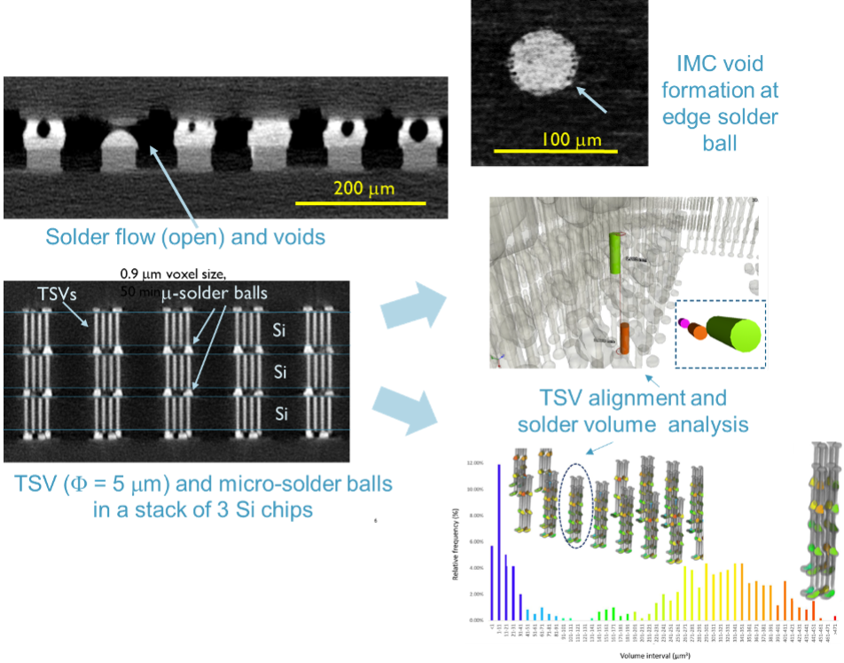
In 3D-technology, several thinned Si chips or even full wafers are stacked on top of each other and electrically interconnected with micro-solder balls and through Si vias (TSVs). XCT can be used to control the bonding and alignment of the stacked chips, without the need for destructive cross-sectioning. When electrical failures are detected such as opens or shorts, XCT can help to locate the failure site and cause. Typical failure signatures that can be visualized by XCT are voids, cracks, solder bridging (shorts), misalignment and delamination.